PCB Layout Review Checklist
Warning. This is a work in progress.
After many years of designing circuit boards, this is my working list when doing a final review of PCB layout. I design boards with microcontrollers so the list is skewed to that end.
See the Schematic Checklist
-
Proper layout of decoupling capacitors - add pictures
-
Optimize layout of oscillators
-
Minimize breaks in ground plane (especially from vias) - add pictures
-
No traces on ground plane breaks - add pictures
-
Extra clearance around high speed signals
-
Impedance on transmission lines
-
Add fiducials
-
Silkscreen clarity
-
Copyright on silkscreen
-
Version on silkscreen
-
Layer stackup
-
Terminate the USB shield
-
Ensure FETs are in a known state at startup (before firmware is driving them)
-
Leave 1mm of no copper on edges of board
-
Export 3D model and check for interferences
-
Review new footprint sizes and pinout against the datasheet
-
Tent all vias
-
Ground pour top and bottom
-
Add teardrops
-
Add ground via near signal via stubs
-
Check trace length matching for high speed signals
-
Minimize parallel run lengths between signals
- Make signal spacing larger than the distance to the ground plane
- Avoid mutual inductance and mutual capacitance
-
Minimizing reflection:
- Use series termination resistor and place near the source point. The series termi-nation resistor should be placed within 1/6th wavelength of the switching speed of the driver.
-
Ringing driver and receiver distance > 1/4 the wavelength
-
What should the target signal rise/fall times be?
-
Prefer daisy chaining to trace branching
-
Proper terminating resistors at the source.
-
Sierra Circuits better DFM (protoexpress.com)
-
Place ferrite disks on top of high speed ICs. The disks are available with adhesive and are easy to add.
For 6 layers or more
- Add ground via nears tracks that change ground reference planes
EMC Specific
- Avoid overlapping clock harmonics
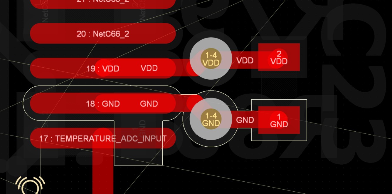
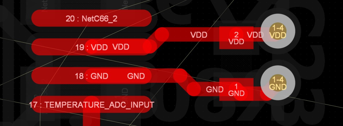
- Decoupling Capacitors should be as close to the power pins as posssible using traces that are as short as possible.
- The capacitor package size has a bigger impact on its ability to filter higher frequencies than the capacitance value
Use this:

Not that:

-
Routing of clock lines and high speed lines should be the shortest and most well-routed traces.
-
No T’s in high speed lines
-
Low speed lines going off the PCB should have ferrites for filtering
-
High speed traces must be on a layer adjacent to a plane
-
Recede the edges of the power plane by 20 times the distance to an adjacent ground plane
-
Avoid slots in power and ground planes
-
Series resistor terminate clock signals to slow rise/fall times
-
Place clocks and circuitry as far away from IO as possible
-
All I/O cables are antennas
-
Below 100KHz DC resistance dominates the return path
-
Above 100KHz current follows plane below trace. If the trace doesn’t have a plane, a loop antenna is created
-
Avoid parasitic coupling: ie routing a cable over an MCU
-
Power input connected shoud all have RF capacitors
-
Place all I/O connectors (including power) on the edge of the board
-
Aim for prototypes to be 6dB below spec to ensure all productions units are passing
-
FCC Measurements are made with a bandwidth in the range of 150 KHz
-
All traces whose length (in inches) is equal to or greater than the signal rise/fall time (in nanoseconds) must have provision for a series-terminating resistor (typically 33 ohms).
-
Above 25 MHz PCB’s should have two (or more) ground planes.
-
Traces as transmission lines
-
Traces as antennas
